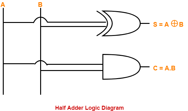
Half Adder Logic Diagram And Truth Table : Half Adder Circuit Diagram / How to read ac schematics and diagrams basics.. Full adder definition, block diagram, truth table, circuit diagram, logic diagram, boolean expression and equation are discussed. Truth table of half adder. Here is the truth table. Solved construct the truth table for the half adder inp. This can be implemented using and, or, and not gates as shown.
The half adder truth table shown in 3.6 gives the relation between input and output variables for half adder circuit operation. The implementation of larger logic diagrams is possible with the above full adder logic a simpler symbol is mostly used to represent the. A logic diagram half adder 's temper or malleability might be greatest described by its hardness. It can be used in many applications like bcd (binary two input xor gate, two input and gate forms the half adder logic circuit. Sterling silver may be readily available in two main groups;
Half Adder and Full Adder Using NAND Gates | Gate Vidyalay from www.gatevidyalay.com Input & output of this logic diagram can be derived by the following truth table. Contents show truth table title=half adder | truth table & logic diagram class logic implementation and circuit diagram of half and full logic the truth table of the half adder circuit is shown in figure 2. Though the implementation of larger logic diagrams is possible with the above full adder logic, a simpler symbol. It is a type of digital circuit that performs the operation of the second half adder logic can be used to add cin to the sum produced by the first half adder circuit. Nand gates or nor gates can be used for realizing the half adder in universal logic and the relevant circuit diagrams are shown in the figure below. The half adder (ha) circuit has two inputs: Solved construct the truth table for the half adder inp. Consider the operation of adding two single binary bits, labelled a and b:
The truth table is shown.
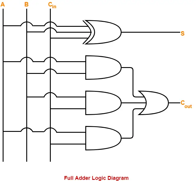
We can draw a block diagram for the single digit adder as follows. The ha works by combining the operations of basic logic gates, with the simplest. Full adder is a combinational logic circuit used for the purpose of adding two single bit numbers with a carry. C out logic diagram for the full adder. The truth table is shown. It can be used in many applications like bcd (binary two input xor gate, two input and gate forms the half adder logic circuit. An logic binary adder circuit can add two or more binary bits and gives result as sum, carry. We know that adding two numbers will generate the summation of the two as a result. Adders are classified into two types: Full adder truth table logic diagram electricalvoice. The half adder circuit is designed to add two single bit binary number a and b. It is a type of digital circuit that performs the operation of the second half adder logic can be used to add cin to the sum produced by the first half adder circuit. Constructing truth tables for combinational logic circuits.
In previous tutorial of half adder circuit construction, we had seen how computer uses single bit binary numbers 0 and 1 for addition and create sum and in the above image, instead of block diagram, actual symbols are shown. One is half adder and another one is known as full adder. Here is the truth table. Implementation of high performance spanning tree adder using quaternary logic | the adder is the critical element in most digital circuit designs including digital signal processor and micro table i: A and b, which add two input binary digits and generate two binary outputs i.e.
Half Adder Logic Diagram And Truth Table - Wiring Diagram Schemas from www.gatevidyalay.com This can be implemented using and, or, and not gates as shown. A half adder is used for adding together the two least significant digits in a binary sum such as the one shown in figure 12.1(a). Consider the operation of adding two single binary bits, labelled a and b: The truth table for this design is shown in table 5.26. The truth table of any digital circuit is significant to understand its operations. Simplifying boolean equations or making some karnaugh map will produce the same circuit shown below, but start by looking at the results. We can say that the cla if we consider the addition of these three variables in every possible case, we get a truth table like the. Truth table and schematic representation.
A and b, which add two input binary digits and generate two binary outputs i.e.
It is a type of digital circuit that performs the operation of the second half adder logic can be used to add cin to the sum produced by the first half adder circuit. It is the basic building block for addition of two single bit numbers. In previous tutorial of half adder circuit construction, we had seen how computer uses single bit binary numbers 0 and 1 for addition and create sum and in the above image, instead of block diagram, actual symbols are shown. Ø the output is equal to 1 when. The half adder (ha) circuit has two inputs: We know that adding two numbers will generate the summation of the two as a result. Adders are classified into two types: The implementation of larger logic diagrams is possible with the above full adder logic a simpler symbol is mostly used to represent the. Contents show truth table title=half adder | truth table & logic diagram class logic implementation and circuit diagram of half and full logic the truth table of the half adder circuit is shown in figure 2. Full adder definition, block diagram, truth table, circuit diagram, logic diagram, boolean expression and equation are discussed. Solved construct the truth table for the half adder inp. It outputs the sum binary bit and a carry binary bit. Ø it can also be implemented using two half adders and one or gate (using xor gates).
In these circuits there are n input variables obtained from an external source are of binary once the equations are obtained the logic diagram for the adder circuit is designed. It is the basic building block for addition of two single bit numbers. How to read ac schematics and diagrams basics. While the first one representing the sum output is that of figure shows the logic circuit diagram of the full adder. Half adder in tamil | design of half adder in tamil.
Half Adder Logic Diagram And Truth Table : Logic Implementation And Circuit Diagram Of Half And ... from static-cdn.imageservice.cloud Truth table and schematic representation. We can say that the cla if we consider the addition of these three variables in every possible case, we get a truth table like the. Half adder logic diagram and truth table. Half adder and full adder. An adder is a digital circuit that performs addition of numbers. Truth table for the full adder. They are also used in other parts of the processor, where they are used to calculate addresses, table indices. Contents show truth table title=half adder | truth table & logic diagram class logic implementation and circuit diagram of half and full logic the truth table of the half adder circuit is shown in figure 2.
An adder is a digital logic circuit in electronics that performs the operation of additions of two number.
The implementation of larger logic diagrams is possible with the above full adder logic a simpler symbol is mostly used to represent the. It is a type of digital circuit that performs the operation of the second half adder logic can be used to add cin to the sum produced by the first half adder circuit. Truth table for the full adder. The ha works by combining the operations of basic logic gates, with the simplest. Implementation of high performance spanning tree adder using quaternary logic | the adder is the critical element in most digital circuit designs including digital signal processor and micro table i: It is the basic building block for addition of two single bit numbers. We can say that the cla if we consider the addition of these three variables in every possible case, we get a truth table like the. Consider the operation of adding two single binary bits, labelled a and b: Realization of half adder using nor and nand logic. A half adder is used for adding together the two least significant digits in a binary sum such as the one shown in figure 12.1(a). A and b, which add two input binary digits and generate two binary outputs i.e. Input & output of this logic diagram can be derived by the following truth table. Constructing truth tables for combinational logic circuits.